- What is Microprocessor?
It is an integrated computer circuit that performs all the arithmetic, logical, data transfer and control functions of a CPU. - Introduction to 8085 Microprocessor
In 1977, Intel Corporation introduced an upgraded version of microprocessor 8080-the 8085. It was last and most successful 8 bit general purpose microprocessor developed by Intel. The main advantages of 8085 were its internal clock generator, internal system controller, and higher clock frequency. Higher level of component integration reduced 8085's cost and increased it's usefulness.


- Architecture of 8085 Microprocessor
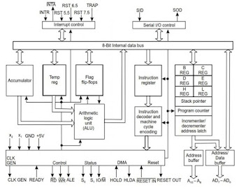 • Components of 8085 Microprocessor
1. Accumulator
2. Temporary Register
3. Registers
4. ALU
5. Flag Registers
6. Instruction Register
7. Instruction Decoder
8. Program Counter
9. Stack Pointer
10. Timing And Control Unit
11. Serial Input And Output Control
12. Interrupt Unit• Functions of the content of Microprocessor
• Accumulator:
It is a 8-bit register which is used to perform arithmetical and logical operation. It stores the output of any operation.• Temporary Register:
It is a 8-bit register which is used to hold the data on which the accumulator is computing operation. It is also called as operand register because it provides operands to ALU.• Registers:
These are general purposes registers. Microprocessor consists 6 general purpose registers of 8-bit each named as B, C, D, E, H and L. Generally theses registers are not used for storing the data permanently. It carries the 8-bits data. These are used only during the execution of the instructions . These registers can also be used to carry the 16 bits data by making the pair of 2 registers . The valid register pairs available are BC, DE, HL. We cannot use other pairs except BC, DE and HL. These registers are programmed by user.• ALU:
It performs the arithmetic operations and logical operation.• Flag Registers:
It consists of 5 flip flop which changes its status according to the result stored in an accumulator. It is also known as status registers. It is connected to the ALU .・There are five flip-flops in the flag register are as follows:
1. Sign (S)- If MSB of the result is 1 then sign flag is set otherwise reset. If sign flag is 1: the number is negative . If sign flag is 0: the number is positive.
2. Zeros (Z)- If the result stored in an accumulator is zero then this flip flop is set otherwise it is reset.
3. Auxiliary carry (AC)- If any carry goes on 4th bit in the output then it is set otherwise it is reset.
4. Parity (P)- If the no of 1's is even in the output stored in the accumulator then it is set otherwise it is reset for the odd.
5. Carry (C)- If the result stored in an accumulator generates a carry in its final output then it is set otherwise it is reset.• Instruction register (IR):
It is a 8-bit register. When an instruction is fetched from memory then it is stored in this register.• Instruction Decoder:
Instruction decoder identifies the instructions. It takes the information's from instruction register and decodes the instruction to be performed.• Program Counter:
It is a 16 bit register used as memory pointer. It stores the memory address of the next instruction to be executed. So we can say that this register is used to sequencing the program.• Stack Pointer:
It is also a 16 bit register used as memory pointer. It points to the memory location called stack. Generally stack is a reserved portion of memory where information can be stores or taken back together.• Timing and Control Unit:
It provides timing and control signal to the microprocessor to perform the various operations.
It has three control signal. It controls all external and internal circuits.
It operates with reference to clock signal.
It synchronizes all the data transfers.• There are three control signal:
1. ALE-Arithmetic Latch Enable, It provides control signal to synchronize the components of microprocessor.
2. RD- This is active low used for reading operation.
3. WR-This is active low used for writing operation.
There are three status signal used in microprocessor S0, S1 and IO/M. It changes its status according the provided input to these pins.• Serial Input Output Control:
There are two pins in this unit. This unit is used for serial data communication.• Interrupt Unit:
There are 6 interrupt pins in this unit. Generally an external hardware is connected to these pins. These pins provide interrupt signal sent by external hardware to microprocessor and microprocessor sends acknowledgement for receiving the interrupt signal. Generally INTA is used for acknowledgement. Pin Diagram of 8085 Microprocessor:

1. Power supply and Clock frequency signals
• Vcc (Pin no.- 40): + 5 volt power supply
• Vss (Pin no.- 20) : Ground
• X1, X2 (Pin no.- 1,2) : Crystal or R/C network or LC network connections to set the frequency of internal clock generator. The frequency is internally divided by two. Since the basic operating timing frequency is 3 MHz, a 6 MHz crystal is connected externally.
• CLK (output) (Pin no.- 37) :Clock Output is used as the system clock for devices interfaced with the microprocessor.2. Address Bus: A8 - A15 (output; 3-state)
(Pin nos.- 21 to 28)
• It carries the most significant 8 bits of the memory address or the 8 bits of the I/O address.3. Address/ Data bus: AD0 - AD7 (input/output; 3-state)
(Pin nos.- 12 to 19)
• These multiplexed set of lines used to carry the lower order 8 bit address as well as data bus.
• During the opcode fetch operation, in the first clock cycle, the lines deliver the lower order address A0 - A7.
• In the subsequent IO / memory, read / write clock cycle the lines are used as data bus.
• The CPU may read or write out data through these lines.4. Control and Status signals
• ALE (output) - Address Latch Enable (Pin no.- 30)
It is an output signal used to give information of AD0- AD7 contents.
It is a positive going pulse generated when a new operation is started by uP.
When pulse goes high it indicates that AD0-AD7 are address.
When it is low it indicates that the contents are data.
• RD (output 3-state, active low) (Pin no.- 32)
Read memory or IO device.
This indicates that the selected memory location or I/O device is to be read and that the data bus is ready for accepting data from the memory or I/O device.
• WR (output 3-state, active low) (Pin no.- 31)
Write memory or IO device.
This indicates that the data on the data bus is to be written into the selected memory location or I/O device.
• IO/M (output) - Select memory or an IO device (Pin no.- 34)
This status signal indicates that the read / write operation relates to whether the memory or I/O device.
It goes high to indicate an I/O operation.
It goes low for memory operations.5. Status Signals S0 – S1 (Pin no.- 29 and 33)
• It is used to know the type of current operation of the microprocessor.6. Interrupts and externally initiated operations
• They are the signals generated by an external device to request the microprocessor to do a particular task or work.
• There are five hardware interrupts called,
TRAP (Pin no.- 6)
RST 7.5 (Pin no.- 7)
RST 6.5 (Pin no.- 8)
RST 5.5 (Pin no.- 9)
INTA (Pin no.- 11)
• On receipt of an interrupt, the microprocessor acknowledges the interrupt by the active low INTA (Interrupt Acknowledge) signal.
• Reset In (input, active low) (Pin no.- 36)
This signal is used to reset the microprocessor.
The program counter inside the microprocessor is set to zero.
The buses are tri-stated.
• Reset Out (Output) (Pin no.- 3)
It indicates CPU is being reset.
Used to reset all the connected devices when the microprocessor is reset.7. Direct Memory Access (DMA): Tri state devices
• When 2 or more devices are connected to a common bus, to prevent the devices from interfering with each other, the tri state gates are used to disconnect all devices except the one that is communicating at a given instant.
• The CPU controls the data transfer operation between memory and I/O device. Direct Memory Access operation is used for large volume data transfer between memory and an I/O device directly.• HOLD (Pin no.- 39) : This signal indicates that another master is requesting the use of the address and data buses.
• HLDA(Pin no.- 38): It indicates that CPU has received the HOLD request . HLDA is set to low after the HOLD signal is removed.
• READY (input) (Pin no.- 35)
Memory and I/O devices will have slower response compared to microprocessors.
Before completing the present job such a slow peripheral may not be able to handle further data or control signal from CPU.
The processor sets the READY signal after completing the present job to access the data.
The microprocessor enters into WAIT state while the READY pin is disabled.8. Single Bit Serial I/O ports
• SID (input) (Pin no.-5): Serial input data line
• SOD (output) (Pin no.-4 ): Serial output data line
These signals are used for serial communication.
This was detail information about 8085 Microprocessor structure.If you are interested to know on any other subject in which you are interested or if you have any doubts then tell us in comment about it.
De-multiplexing of AD0-AD7 in 8085 Microprocessor
https://facts-updates.blogspot.com/2020/12/8085-microprocessor-de-multiplexing-of.html


Comments
Post a Comment